
Dark Factories for Optical Manufacturing
Alexander Lange / Nov 12, 2026

TL;DR
AI can design optical parts faster than anyone can make and test them. Verified physical results are the bottleneck now
Optics splits design from fabrication. The two standard design tools date from 1975 and 1990 and belong to two incumbents, Keysight and Synopsys, which sell seats. Fabs file their measurements in QA folders; fabrication data is not integrated into the design process
A dark fab closes the loop: spec, AI design, simulation, printing without moulds, and metrology on every part. Every deviation retrains the model.
The open gap is small batches, between catalogue houses and mass moulders: defence, aerospace, medical devices, photonics prototypes. The US defense bill now pushes those buyers to domestic suppliers.
Opdo is building a neutral foundry for optics, inspired by the TSMC model. It raised a $2.3M pre-seed led by Angular Ventures, with Inflection and Tiny.
 Subscribe
Why we backed Opdo
AI can simulate the physical world increasingly well. Human verification and data-feedback loops from the physical world have become the critical bottlenecks for improving production. We can overcome them by automated factories (dark factories) that are equipped with cameras and sensors to measure every part and every step of the value chain. Such data is then fed back into the AI models to improve simulations.
We have seen this model work out for material sciences during a visit of Radical's pilot lab in NYC in early 2026 and see it applied in various industries. Optical engineering and manufacturing is one where we see vast potential given the industry's market structure and strong macro tailwinds from photonic computation.
how optical engineering works
Optical manufacturing is a subtractive process used to create components like lenses, mirrors, prisms, and filters from raw materials such as optical glass, crystals, or specialized plastics. An optical engineer turns a requirement into a part that can be built, then proves it works. Broken down into five steps it looks like this:
1/ Specification. The customer states what the light must do. E.g. focus a laser to a point, spread it into a line, or image a scene at a set resolution.
2/ Design. The engineer picks the surfaces, the materials and the spacing between them. What follows is the prescription: every curvature, thickness and material type is defined. Many modern parts use aspheres, surfaces that are not slices of a sphere. Some use freeforms, which have no symmetry at all.
3/ Simulation. Software runs a ray trace (simulation that tracks the exact path of light rays through an optical system). It follows thousands of light rays through each surface and bends each one by Snell's law of refraction. Where the rays fail to meet at one point, the design has aberrations, the optical word for built-in blur. The usual score is the spot size, the width of the patch where the rays land.
4/ Tolerancing. No factory hits a prescription exactly. A tolerance is the error allowed on each number, such as a curvature within ±0.5%. A tolerance run rebuilds the design thousands of times in software with random errors. It counts how many copies still meet spec. That share is the expected yield. Tighter tolerances raise yield and cost.
5/ Fabrication and metrology. The shop grinds and polishes glass, cuts, moulds or prints it. Metrology then measures the finished part's shape and performance against the simulation.
Each step has its own specialist and often its own company. A design that fails in metrology goes back to the start.
the verification bottleneck
In physical engineering, ideas and simulations are abundant. Verified and repeatable physical outcomes are rare. A generative model can propose thousands of candidate designs in a day. Each one still has to be made, measured and compared against the simulation. That step runs at the speed of a lab or a factory.
Optics show this problem in a sharp form. Precision optical components such as lenses, mirrors, and micro-optics sit at the physical interfaces where light is generated, steered, coupled, or detected. They act as the critical bridges connecting lasers, silicon chips, optical fibers and sensors in several of the world's largest photonic and semiconductor markets: photonic chips, packaging and lithography, optical switches, VR AR, LiDAR and many more.
A custom part needs a design, a quote, often tooling, and finally fabrication. Vendors advertise custom production times of four to six weeks for volume orders. Prototypes that miss a spec go back to square one.
Design is the second queue. The field has a documented shortfall of optical engineers, especially in the US and Europe. Every hardware team needs a few of them. Few teams have one.
status quo: design and production are decoupled
The industry split design from fabrication, so data from real parts never reaches the designer directly. The tooling landscape is consolidated and outdated: CODE V launched commercially in 1975 and Zemax launched in 1990. Both automate the evaluation of a design and sit with two incumbents. Keysight acquired CODE V from Synopsys in October 2025, and Zemax sits with Synopsys via Ansys. Both sell seats. Revenues grow with the number of human optical designers using their software.
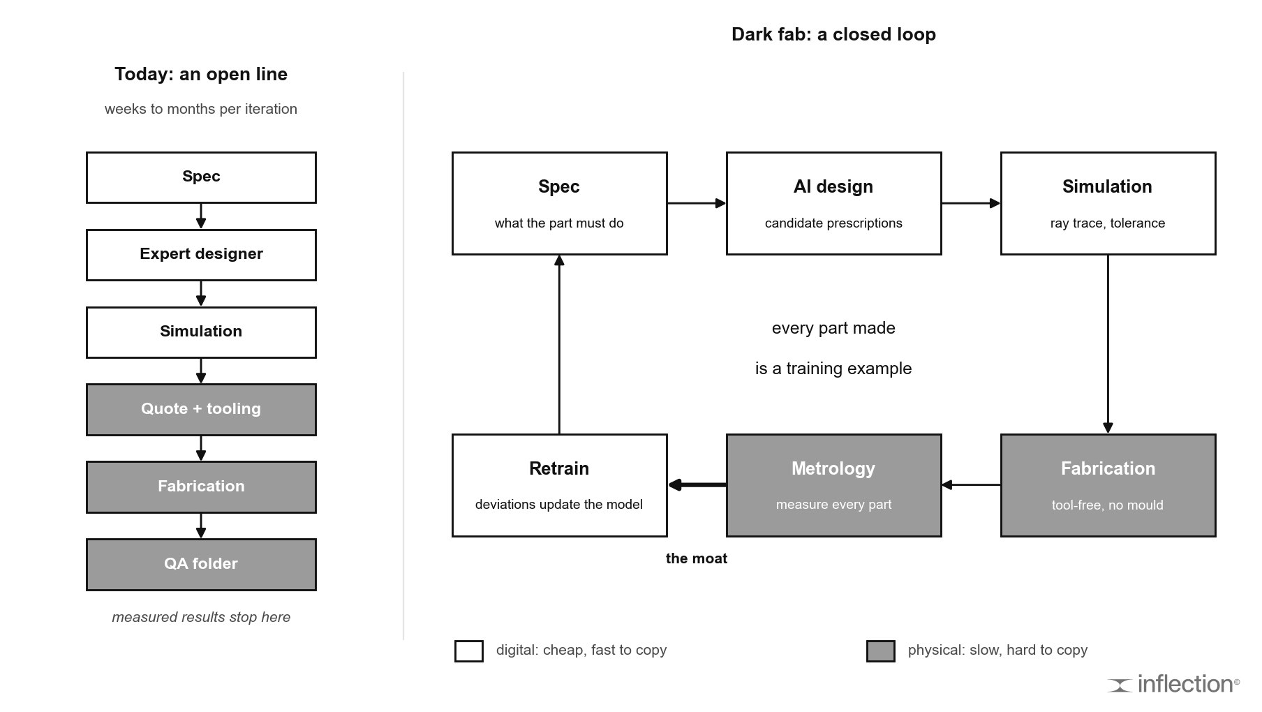
The fabs are producing in isolation. Each runs its own process, machines and quality checks. When a finished lens deviates from the simulation, the measurement lands in a QA folder. Each new project starts from the same priors as the last - there are no data network effects across design and manufacturing.
future: optical dark fabs that teach AI models
A dark fab runs spec, AI design, simulation, fabrication and metrology in one loop, lights off. The loop would look like this:
customers state what the part must do
the model proposes candidate prescriptions and ranks them in simulation
tool free print of the part, no mould and no grinding
metrology measures every part against the simulation
deviations are fed back into the design model
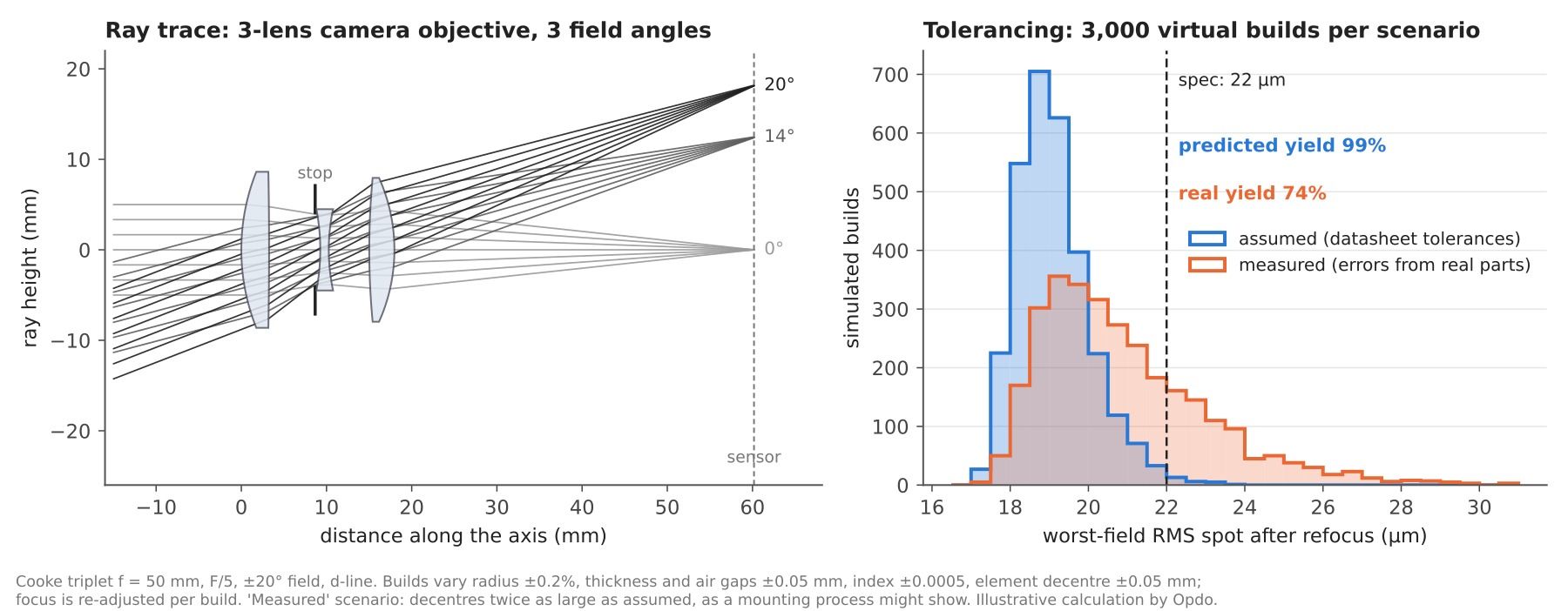
The simulation runs on assumptions. The figure above (left) traces rays through a three-lens camera objective. It then rebuilds the lens 3,000 times with typical shop tolerances. With datasheet tolerances, 99% meet spec; if the real process decentres the lenses twice as much as assumed, only 74% do. The error ranges in a run like this are guesses taken from a datasheet. A fab that measures every part can replace the guesses with its own measured errors. That is the critical data the loop feeds back.
The printing step can be accelerated with novel technology too. Xolography cures resin where two light beams cross. Processes like this make a one-off freeform lens as cheap to start as the thousandth. The Opdo founders were previously part of the Xolo team, the company that invented and deployed Xolography for the first time.
At Inflection we've seen the pattern in other fields. At Radical we enjoyed a tour through their first dark fab prototype in Manhattan. It makes and characterizes more than 25 alloys a day and indexes every failed experiment for the next prediction. Its output was orders of magnitude above a conventional materials group. Recursion runs up to 2.2 million biology experiments a week in its automated labs. Every single one of them trains its underlying models.
market opportunity
The market for precision optics is large and sits somewhere between $21BN to about $32 BN today, depending on definitions and expected to grow towards $50BN to $100BN by 2035 (same sources) with CAGRs around ~8-12%.
The market's gap seems to sit in the middle of the volume curve. Catalogue houses sell standard parts in days but don't customize. Mass producers mould millions of identical lenses for phones and cars because tooling only pays at large volumes. Small batches around tens of thousands of units seem to fall between the cracks. Defence, aerospace, medical devices, scientific instruments, photonic chips / packaging prototypes fall into this category. Buyers are willing to pay for speed and precision.
Supply chain security and China dependency are motivating the re-shoring of critical industries, including optics. The US defense bill now restricts optics from "covered nations". Defense primes and other critical industries need domestic sources for parts they used to import. A domestic fab with a short loop is the obvious answer to that challenge.
We currently think that a vertically integrated approach makes most sense for a venture scale business. Selling seats (software) or designs (IP) are the logical first steps to roll out products and services but only the production of optical parts yields maximal leverage of a "full loop" system as described above. This is Opdo's long term ambition.
investment thesis
Three intersecting developments are unlocking dark fabs for optical manufacturing: (1) AI cuts the cost and increases the volume of design, (2) new fabrication methods cut the cost of custom parts, (3) supply chain security is repricing the category for critical high tech industries in the west.
The end state is a foundry model, inspired by TSMC. TSMC was founded in 1987 as a pure foundry. Its guiding principle since then was to "not compete with customers" on end user electronics like Samsung, Sony, Apple and others did for decades. Instead, chip designers handed it their most sensitive designs because it would never sell a rival chip. Integrated chip producers that also sold their own chips couldn't escape that conflict. The result for TSMC were unprecedented economies of scale and extreme depth of process knowledge.
Optics has a somewhat comparable market structure to that of the semiconductor industry of the 1980s. Materials, design tools, equipment, fabrication, assembly. Synopsys and Keysight hold the design tools, equipment makers such as Xolo play ASML's part. The free-space optics branch has no neutral foundry yet. Enter Opdo.
Opdo is building that foundry for optics. It is an AI-native optical engineering company in Los Angeles. Its agents work inside Zemax and CODE V, so engineers keep their tools. Its own engineers deliver design projects, and customers can source prototypes and finished parts through the company. Data from manufactured and tested parts feeds back into its models. Projects already cover laser and imaging systems, micro-optics and nanostructured surfaces.
The founders have done this before. CEO Stephan Kuehr co-founded 3YOURMIND, whose software automates distributed manufacturing for customers including the US Department of Defense, Ford and Bosch. CTO Yousef Arzhangnia modeled Xolo's volumetric printing process end to end and built physics-informed ML for shape fidelity. His background spans optical engineering, AI and automation.
The company just announced its $2.3M pre seed led by Angular Ventures, with Inflection and Tiny participating. Reach out if you would like to collaborate.
#optics#photonics#dark factory#manufacturing#physical AI#AI design#metrology
Related
Subscribe